ADT7463
http://onsemi.com
14
ADT7463 Read Operations
The ADT7463 uses the following SMBus read protocols.
Receive Byte
This is useful when repeatedly reading a single register.
The register address needs to have been set up previously. In
this operation, the master device receives a single byte from
a slave device as follows:
1. The master device asserts a start condition on SDA
2. The master sends the 7bit slave address followed
by the read bit (high)
3. The addressed slave device asserts ACK on SDA
4. The master receives a data byte
5. The master asserts NO ACK on SDA
6. The master asserts a stop condition on SDA and
the transaction ends
In the ADT7463, the receive byte protocol is used to read
a single byte of data from a register whose address has
previously been set by a send byte or write byte operation.
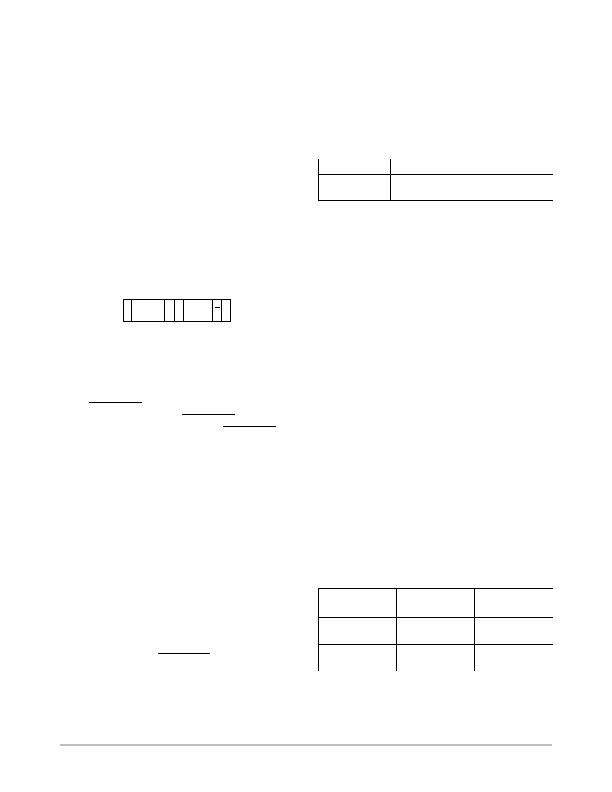
Figure 22. Single Byte Read from a Register
SLAVE
ADDRESS
DATA
A
R
S
A P
2
4
3
1
5 6
Alert Response Address
Alert response address (ARA) is a feature of SMBus
devices that allows an interrupting device to identify itself
to the host when multiple devices exist on the same bus.
The SMBALERT
output can be used as an interrupt
output or can be used as an SMBALERT
. One or more
outputs can be connected to a common SMBALERT
line
connected to the master. If a devices SMBALERT
line goes
low, the following procedure occurs:
1. SMBALERT
is pulled low
2. Master initiates a read operation and sends the
alert response address (ARA = 0001 100). This is
a general call address that must not be used as a
specific device address
3. The device whose SMBALERT
output is low
responds to the alert response address, and the
master reads its device address. The address of the
device is now known and it can be interrogated in
the usual way
4. If more than one devices SMBALER
T output is
low, the one with the lowest device address will
have priority in accordance with normal SMBus
arbitration
5. Once the ADT7463 has responded to the alert
response address, the master must read the status
registers and the SMBALERT
will only be cleared
if the error condition has gone away
SMBus Timeout
The ADT7463 includes an SMBus timeout feature. If
there is no SMBus activity for 35 ms, the ADT7463 assumes
that the bus is locked and releases the bus. This prevents the
device from locking or holding the SMBus expecting data.
Some SMBus controllers cannot handle the SMBus timeout
feature, so it can be disabled.
Table 6. CONFIGURATION REGISTER 1 (REG. 0X40)
Bit
Description
<6> TODIS
0: SMBus Timeout Enabled (Default)
<6> TODIS
1: SMBus Timeout Disabled
Voltage Measurement Inputs
The ADT7463 has four external voltage measurement
channels. It can also measure its own supply voltage, V
CC
.
Pins 20 to 23 are dedicated to measuring 5 V, 12 V, and
2.5 V supplies and the processor core voltage V
CCP
(0 V to
3 V input). The V
CC
supply voltage measurement is carried
out through the V
CC
pin (Pin 4). Setting Bit 7 of
Configuration Register 1 (Reg. 0x40) allows a 5 V supply to
power the ADT7463 and be measured without overranging
the V
CC
measurement channel. The 2.5 V input can be used
to monitor a chipset supply voltage in computer systems.
AnalogtoDigital Converter (ADC)
All analog inputs are multiplexed into the onchip,
successive approximation, ADC. This has a resolution of
10 bits. The basic input range is 0 V to 2.25 V, but the inputs
have builtin attenuators to allow measurement of 2.5 V,
3.3 V, 5 V, 12 V, and the processor core voltage V
CCP
without any external components. To allow for the tolerance
of these supply voltages, the ADC produces an output of 3/4
full scale (decimal 768 or 300 hex) for the nominal input
voltage and so has adequate headroom to cope with
overvoltages.
Input Circuitry
The internal structure for the analog inputs is shown in
Figure 23. Each input circuit consists of an input protection
diode, an attenuator, plus a capacitor to form a firstorder,
lowpass filter that gives the input immunity to high
frequency noise.
Table 7. VOLTAGE MEASUREMENT REGISTERS
Register
Description
Default
0x20
2.5 V Reading
0x00
0x21
V
CCP
Reading
0x00
0x22
V
CC
Reading
0x00
0x23
5 V Reading
0x00
0x24
12 V Reading
0x00
发布紧急采购,3分钟左右您将得到回复。
相关PDF资料
ADT7476AARQZ-R
IC REMOTE THERMAL CTLR 24QSOP
ADT7481ARMZ-1RL
IC SENSOR TEMP 2CH ALARM 10MSOP
ADT7482ARMZ-REEL
IC SENSOR TEMP 2CH ALARM 10MSOP
ADT7485AARMZ-R
IC TEMP/VOLT DGL SENS SST 10MSOP
ADT7486AARMZ-RL
IC TEMP SENS DGTL 2CH SST 10MSOP
ADT7488AARMZ-RL
IC TEMP/VOLT DGTL W/SST 10MSOP
ADT7518ARQZ
IC SENSOR TEMP QD ADC/DAC 16QSOP
AT30TS00-MAH-T
SENSOR DGTL TEMP I2C/SMBUS 8WDFN
相关代理商/技术参数
ADT7463ARQZ-REEL7
功能描述:IC REMOTE THERMAL CTRLR 24-QSOP RoHS:是 类别:集成电路 (IC) >> PMIC - 热管理 系列:dBCool® 标准包装:1 系列:- 功能:温度监控系统(传感器) 传感器类型:内部和外部 感应温度:-40°C ~ 125°C,外部传感器 精确度:±2.5°C 本地(最大值),±5°C 远程(最大值) 拓扑:ADC,比较器,寄存器库 输出类型:2 线 SMBus? 输出警报:无 输出风扇:无 电源电压:2.7 V ~ 5.5 V 工作温度:-40°C ~ 125°C 安装类型:表面贴装 封装/外壳:SOT-23-8 供应商设备封装:SOT-23-8 包装:Digi-Reel® 其它名称:296-22675-6
ADT7466
制造商:AD 制造商全称:Analog Devices 功能描述:dBCool Remote Thermal Controller and Voltage Monitor
ADT7466ARQZ
功能描述:板上安装温度传感器 RMT THRM CTR VLT MON RoHS:否 制造商:Omron Electronics 输出类型:Digital 配置: 准确性:+/- 1.5 C, +/- 3 C 温度阈值: 数字输出 - 总线接口:2-Wire, I2C, SMBus 电源电压-最大:5.5 V 电源电压-最小:4.5 V 最大工作温度:+ 50 C 最小工作温度:0 C 关闭: 安装风格: 封装 / 箱体: 设备功能:Temperature and Humidity Sensor
ADT7466ARQZ-REEL
功能描述:板上安装温度传感器 RMT THRM CTR VLT MON RoHS:否 制造商:Omron Electronics 输出类型:Digital 配置: 准确性:+/- 1.5 C, +/- 3 C 温度阈值: 数字输出 - 总线接口:2-Wire, I2C, SMBus 电源电压-最大:5.5 V 电源电压-最小:4.5 V 最大工作温度:+ 50 C 最小工作温度:0 C 关闭: 安装风格: 封装 / 箱体: 设备功能:Temperature and Humidity Sensor
ADT7466ARQZ-REEL7
功能描述:IC REMOTE THERMAL CTRLR 16QSOP RoHS:是 类别:集成电路 (IC) >> PMIC - 热管理 系列:dBCool® 标准包装:1 系列:- 功能:温度监控系统(传感器) 传感器类型:内部和外部 感应温度:-40°C ~ 125°C,外部传感器 精确度:±2.5°C 本地(最大值),±5°C 远程(最大值) 拓扑:ADC,比较器,寄存器库 输出类型:2 线 SMBus? 输出警报:无 输出风扇:无 电源电压:2.7 V ~ 5.5 V 工作温度:-40°C ~ 125°C 安装类型:表面贴装 封装/外壳:SOT-23-8 供应商设备封装:SOT-23-8 包装:Digi-Reel® 其它名称:296-22675-6
ADT7466ARQZ-RL7
功能描述:板上安装温度传感器 RMT THRM CTR VLT MON RoHS:否 制造商:Omron Electronics 输出类型:Digital 配置: 准确性:+/- 1.5 C, +/- 3 C 温度阈值: 数字输出 - 总线接口:2-Wire, I2C, SMBus 电源电压-最大:5.5 V 电源电压-最小:4.5 V 最大工作温度:+ 50 C 最小工作温度:0 C 关闭: 安装风格: 封装 / 箱体: 设备功能:Temperature and Humidity Sensor
ADT7466ZEVB
功能描述:BOARD EVALUATION ADT7466 RoHS:是 类别:编程器,开发系统 >> 过时/停产零件编号 系列:dBCool® 标准包装:1 系列:- 传感器类型:CMOS 成像,彩色(RGB) 传感范围:WVGA 接口:I²C 灵敏度:60 fps 电源电压:5.7 V ~ 6.3 V 嵌入式:否 已供物品:成像器板 已用 IC / 零件:KAC-00401 相关产品:4H2099-ND - SENSOR IMAGE WVGA COLOR 48-PQFP4H2094-ND - SENSOR IMAGE WVGA MONO 48-PQFP
ADT7467
制造商:AD 制造商全称:Analog Devices 功能描述:dBCool Remote Thermal Monitor and Fan Controller
